In the past two years, due to out-of-stock and price increases and other factors, many manufacturers through domestic replacement to solve the problem of project shortage, domestic motor driver chip in voltage withstand voltage, current drive ability and anti-static, anti-surge reliability has a good performance, Topdiode TNSG27531 double low side, high current drive can be compatible to replace TI UC27531 chip.
Characteristics of UCC27531
Low cost gate driver (provides the best solution for driving FET and IGBT)
Discrete transistor is an excellent substitute for driver (providing simple interface with controller)
TTL and CMOS compatible input logic threshold (independent of supply voltage)
The split output option enables on and off current regulation.
Inverting and noninverting input configuration Enabled by a fixed TTL compatible threshold.
It has a peak driving pull current of up to 2.5A and a peak driving sink current of 2.5A or 5A at 18V VDD. Wide VDD ranges from 10V to 35V.
The input and enable pins can withstand DC voltage lower than the ground voltage and up to–5v.
When the input is floating or during VDD UVLO, the output remains low. Fast propagation delay (typical 17ns) Rapid rise and fall time (Typical values at 1800pF load are 15ns and 7ns, respectively).
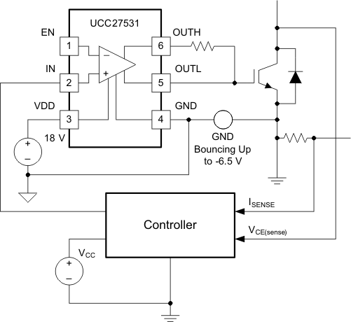
Undervoltage lockout (UVLO) Used as a high-side or low-side driver (if appropriate bias and signal isolation design is adopted).
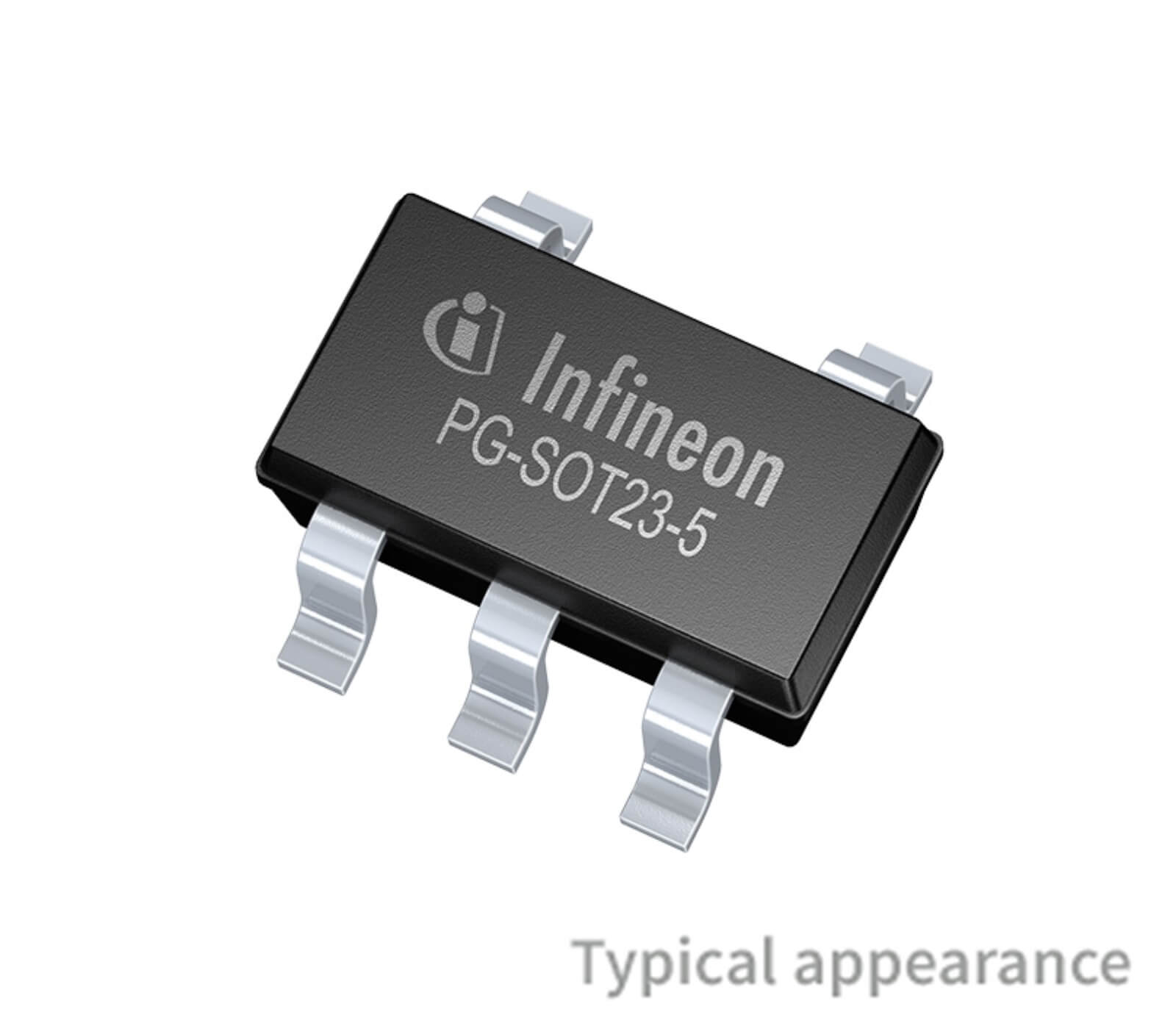
Low-cost, space-saving 5-pin or 6-pin DBV (SOT-23) package options UCC27536 and UCC27537 are pin-to-pin compatible with TPS2828 and TPS2829.
The operating temperature range is–-40°C to 140 C.
Description of UCC27531
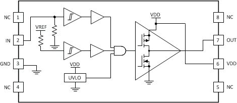
UCC2753x single-channel high-speed gate driver can effectively drive MOSFET and IGBT power switches. UCC2753x device is an ideal solution for MOSFET and IGBT power switches, which adopts a design that provides up to 2.5A and 5A sink current through asymmetric driving (separated output), and combines the functions of supporting negative turn-off bias voltage, rail-to-rail driving function and minimal propagation delay (usually 17ns). UCC2753x series devices can also support enable, dual input and inverting and noninverting input functions. Isolated output and powerful asymmetric driving improve the immunity of the device to parasitic Miller effect and help reduce ground jitter.
Keeping the input pin disconnected will keep the driver output low. The logical behavior of the driver is shown in the application diagram, timing diagram and input and output logic truth table.
The internal circuit on the VDD pin provides an undervoltage lockout function, which keeps the output low until the VDD supply voltage is within the operating range.